In the first step, the delivered wafers are applied on an elastic adhesive film with which it is possible to further handle the wafers in a safe way during the following process steps. Upon customer request we directly return the sawed stretched wafers on frames or in a clamping ring to the customer for further processing. Wafers are typically processed in a size between 4'' to 8''. It also is possible to process wafer segments.
-
 Our technologies for your rapid development success
 -
 Take advantage of our fast and flexible service
 -
 Realize new ideas in dialog with us
Overview of Technologies
In the following, technology steps for the package production are presented. Individual technology steps can quickly and flexibly be adjusted to the package types desired by the customer.
Wafer - stretched wafer
 stretched wafer
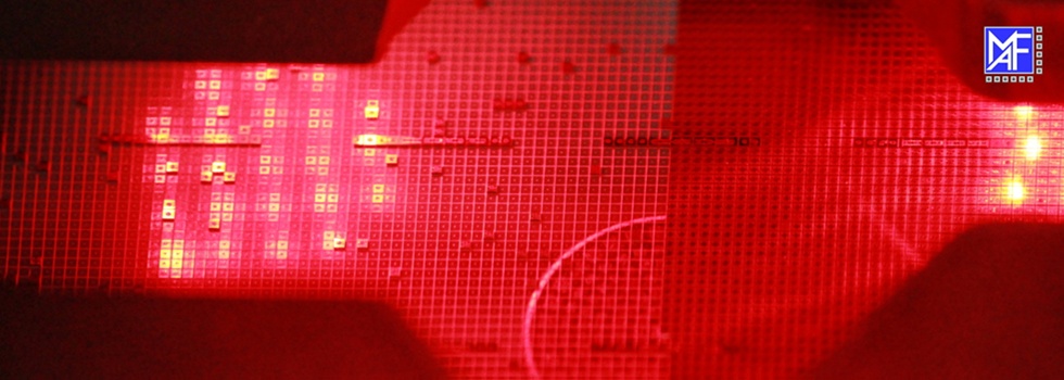
 Wafer - abrasive cutting (Dicing)
 sawed wafer
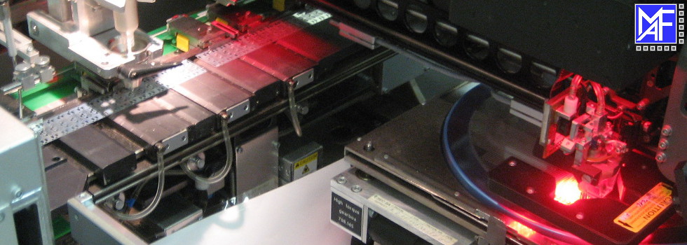
 In the second process step, the wafer is sawed with high-precision. Wafers can subsequently be cleaned with an integrated washing station. The individual DIE's are afterwards separated from one another and can separately be further processed. A processing of wafers up to 8" is possible.
Leadframe
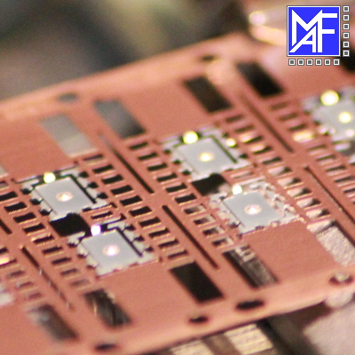 leadframe
 We have most diverse leadframes which can be used for the assembly. Upon customer request, individual developments can also be processed.
Materials for leadframes View less …DIE-Bonding
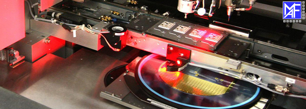
 epoxy adhesive on leadframe
 In the next step, an epoxy adhesive is applied to the leadframe. With the DIE-Bonder the DIE's are fully automatically withdrawn from the 6“- and 8“-frames of the stretched, sawed wafers and attached to the leadframe. Subsequently the epoxy adhesive is hardened in the temperature oven.
Wire-Bonding
 Wire-Bonding
 Wire bonding is executed fully automatically. In general, work is carried out with fine wires of Gold in a thickness between 20µm to 50µm.
Shear- and pull test
 pull test
 For quality control, bonding process is examined during shear- and pull test and a high and consistent quality level is ensured during production.
Molding
 molded leadframe
 After release the leadframe with its bonded DIE's undergoes an insert molding with epoxy resin by use of a multiplunger molding system. The process is fully-automatic.
Marking with laser and Dambar-Cutting
 component marking with laser
 Marking is performed with a fiber laser which is flexibly and quickly programmable for the desired use.
After marking the packages the next step is Dambar-Cutting.
Tin Plating
 leadframe after tinning
 In preparation of Tin Plating the leadframes undergo several steps within our chemistry lab. These include the cleaning, activating, tinning and drying of leadframes. Thereby, processes are strictly monitored in order to enable a constantly high level of quality. Lead-free matt tin is used for the coating.
For the prevention of whisker formation a further tempering takes place after tinning.
Bending and isolation
 bending and isolation
 Bending of electric components and their isolation from the leadframe is fully automated performed on a trim and form machine.
Packing of products
 Products in tube
 The finished components can, upon customer request, be delivered in tubes, trays or in tape & reel. In our delivery terms you will find more details.
MAF
Microelectronic Assembly Frankfurt (Oder) GmbH
Otto-Hahn-Straße 24
15236 Frankfurt (Oder)
Phone: +49 335 3871963
Fax: +49 335 3871964
Mail: info@maf-ffo.com
Flyer